📚 Memory Unit Overview
The memory unit is a collection of storage cells organized with associated circuits for information transfer. Information is stored in groups of bits called words.
Types of Main Memory
Main memory utilizes two major types:
Key Characteristic: Access time is the same regardless of physical location - hence "random access"
Operations: Both Read and Write
Volatility: Data is lost when power is turned off
Key Characteristic: Performs read operations only
Operations: Read only - no write capability
Permanence: Information is determined during hardware production and cannot be altered
⚖️ RAM vs ROM Comparison
| Feature | RAM | ROM |
|---|---|---|
| Full Form | Random-Access Memory | Read-Only Memory |
| Access Type | Random access to any location | Read-only access |
| Write Capability | ✅ Yes - Read & Write | ❌ No - Read only |
| Volatility | Volatile (data lost when power off) | Non-volatile (permanent storage) |
| Access Speed | Uniform - same for all locations | Fast - but read-only |
| Primary Use | Temporary data storage, active programs | Fixed programs, constant tables, firmware |
| Programming | Continuously reprogrammable | Programmed during manufacture or once |
ROM Types
Programmed by the manufacturer during fabrication. Cannot be changed after production.
Uses fusible links that can be "blown" once by the user. Programming is permanent and irreversible.
Can be erased and reprogrammed. EPROM uses UV light for erasing; EEPROM uses electrical signals.
⚙️RAM Chip
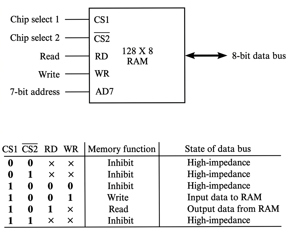
When the chip is selected and the Write signal is active, the data from the Data Bus is transferred into the memory location addressed by AD.
Transfer content of data bus to memory location specified by AD
When the chip is selected and the Read signal is active, the data stored at the memory location addressed by AD is transferred onto the Data Bus.
Transfer content from memory location specified by AD to data bus
The Inhibit State
⚙️ROM Chip
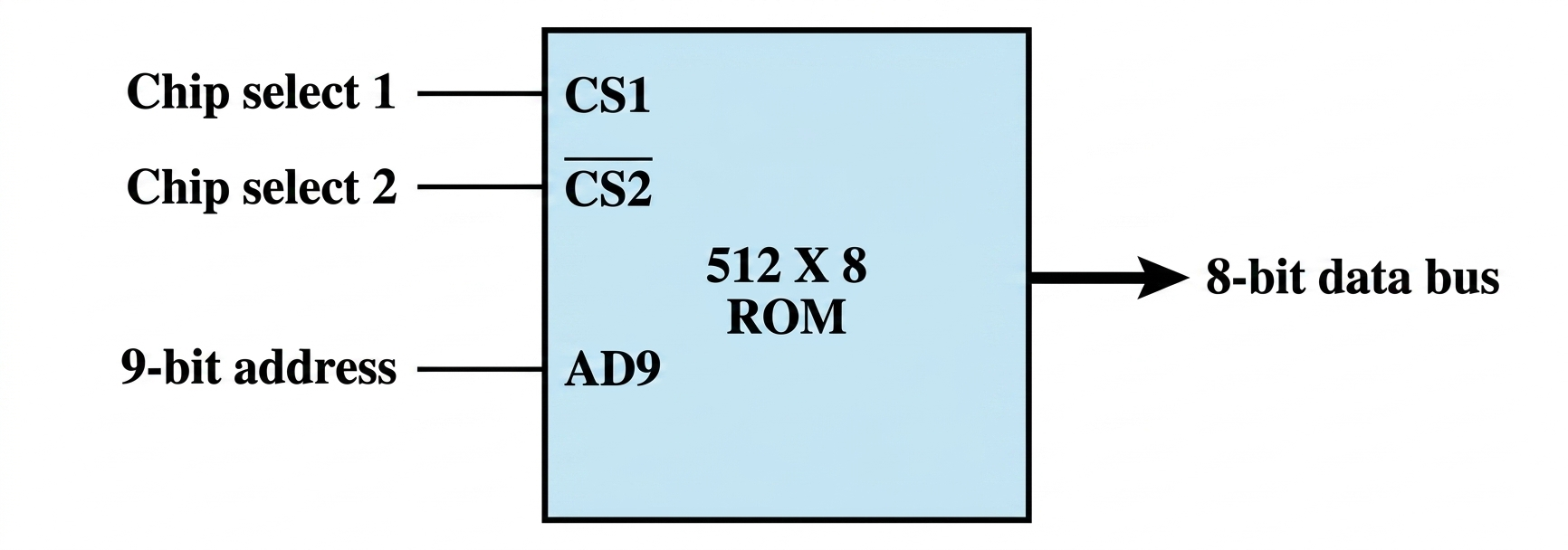
When the chip select conditions are met, the content of the ROM (M) at the 9-bit address (AD) is placed onto the data bus.
The Inhibit State
🧮 Memory Address Map
The address mapping operation for the configuration consisting of 512 bytes each of RAM and ROM is performed as follows:
- Identify Component Requirements
- RAM Capacity: The system uses four RAM chips (RAM1, RAM2, RAM3 and RAM4), each containing 128 bytes. Each chip requires 7 address lines (lines 1 through 7) because 27 = 128.
- ROM Capacity: The system uses one ROM chip containing 512 bytes. This chip requires 9 address lines (lines 1 through 9) because 29 = 512.
- Define the Address Bus Structure
- Total Bus Lines: While the system has a 16-line address bus, this mapping example utilizes only the first 10 lines; the remaining 6 are assumed to be zero.
- Internal Addressing (x): Small 'x's in the address map designate lines connected directly to the address inputs of each chip to select specific bytes within that chip.
- Establish Chip Selection Logic: To distinguish between the different physical chips, higher-order bus lines are assigned as selection bits:
- RAM vs. ROM Selection: Bus line 10 is used to distinguish between RAM and ROM. When line 10 is 0, a RAM chip is selected. When line 10 is 1, the ROM chip is selected.
- Individual RAM Chip Selection: Bus lines 8 and 9 are used to distinguish between the four distinct RAM chips.
- Map the Address Space: The resulting hexadecimal address ranges for each component are determined by these bit assignments:
Component Line 10 (Type) Line 9-8 (Chip ID) Address Range (in Hex) RAM1 0 00 0000 - 007F RAM2 0 01 0080 - 00FF RAM3 0 10 0100 - 017F RAM4 0 11 0180 - 01FF ROM 1 XX 0200 - 03FF By using this map, the designer ensures that the processor can uniquely communicate with each memory component without address overlap.
🔗 Memory-CPU Connection
Interconnection and Operation of a Integrated RAM/ROM Memory System in a CPU Architecture
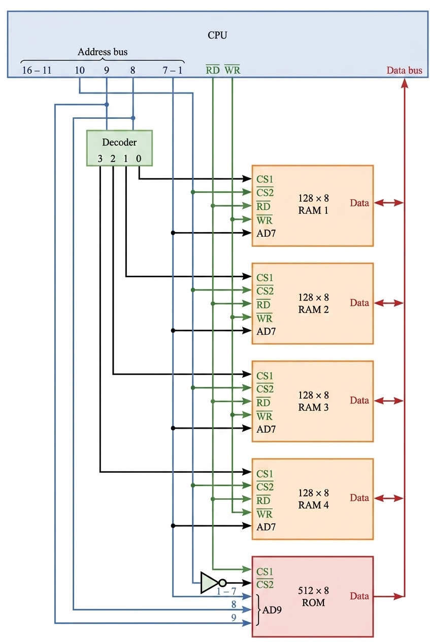
Key Connection
Selection Logic
- RAM Selection: Occurs when address line 10 is 0.
- ROM Selection: Occurs when address line 10 is 1.
- Inhibit State: If a chip is not enabled by the select inputs or control signals, the memory is inhibited and its data bus remains in a high-impedance state to avoid bus contention.
🎮 Interactive Memory Demo
Click on memory cells to simulate read/write operations!