Control Unit Design
Microinstruction Structure
Microinstructions are divided into fields, with each field defining a distinct control function. The key characteristics include:
- Field-based organization: Each field provides control bits to initiate specific microoperations
- Special control bits: Specify how the next address is evaluated
- Branching capabilities: Address fields enable branching within control sequences
- Reduced instruction size: Grouping mutually exclusive variables and encoding k bits provides 2^k microoperations per field
Field Encoding Benefits
By encoding control signals into fields, we achieve:
✓ Reduced Size
Smaller microinstruction bits through field encoding
✗ Added Hardware
Requires decoders external to control memory
⚠ Increased Delay
Decoding through decoder circuit adds time
Example: Three-Field Microinstruction
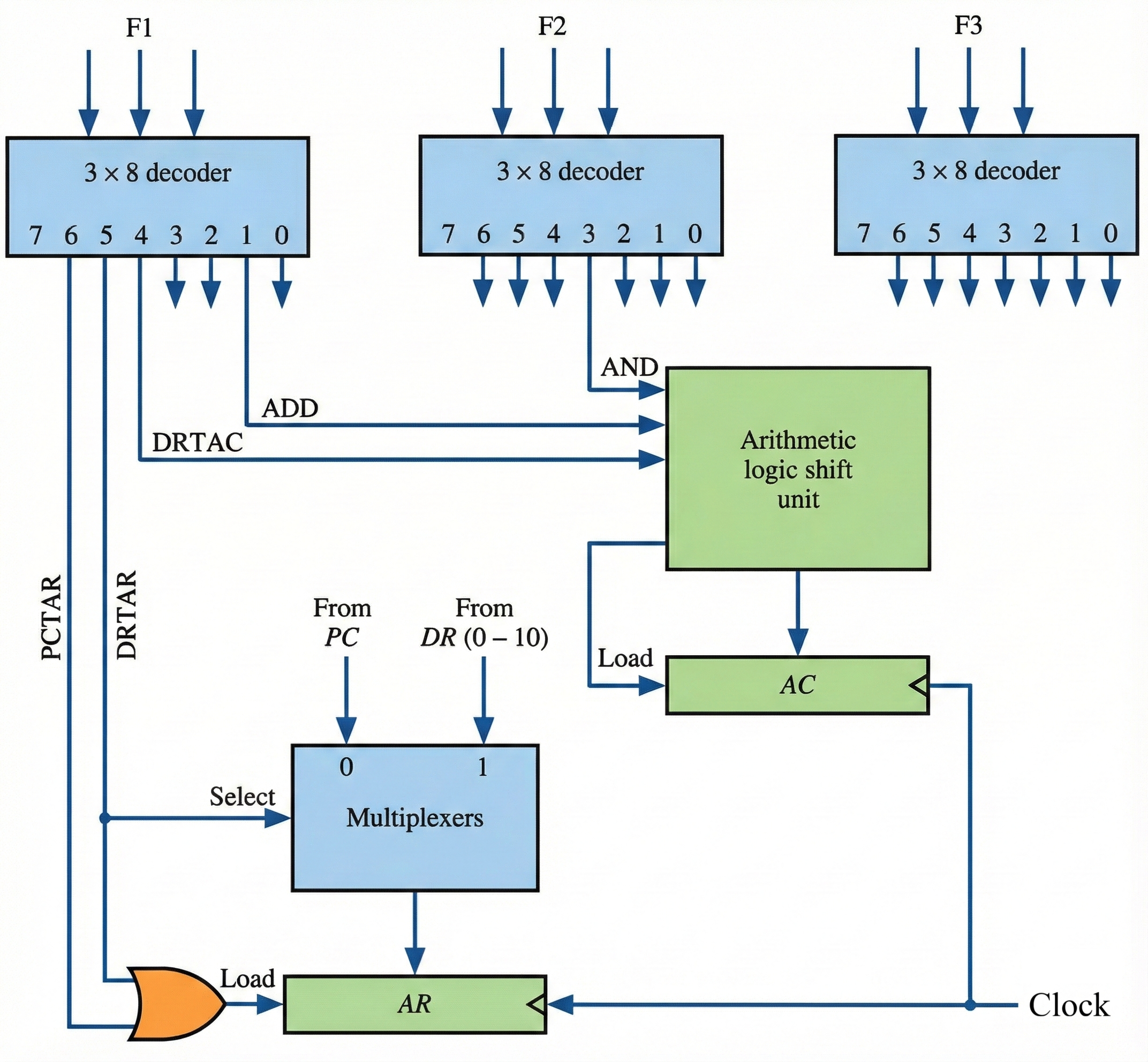
A typical microinstruction can be divided into three subfields of three bits each. The control memory output of each subfield must be decoded to provide distinct microoperations.
With a 3 × 8 decoder, each field provides 8 outputs that must be connected to initiate the corresponding control signals in the processor unit.
Decoder Design & Implementation
Decoder Configuration
Three decoders (F1, F2, F3) process the microinstruction fields. Each 3-bit input produces 8 distinct outputs that control different microoperations.
Interactive Decoder Simulator
Click on the binary digits to toggle them and see which outputs are activated:
Field F1
Field F2
Field F3
Example: F1 = 101 (Binary 5)
When F1 = 101, the next clock pulse transition transfers the content of DR(0-10) to AR. This is symbolized as DRTAR.
Similarly, F1 = 110 initiates a transfer from PC to AR (PCTAR).
Multiplexer Integration
Outputs 5 and 6 of decoder F1 connect to the load input of AR. When either output is active:
- Output 5 active: Multiplexer selects information from DR
- Output 5 inactive: Multiplexer selects information from PC
The transfer to AR occurs with a clock pulse transition only when output 5 or 6 is active.
Circuit Diagram
Microprogram Sequencer
Purpose & Function
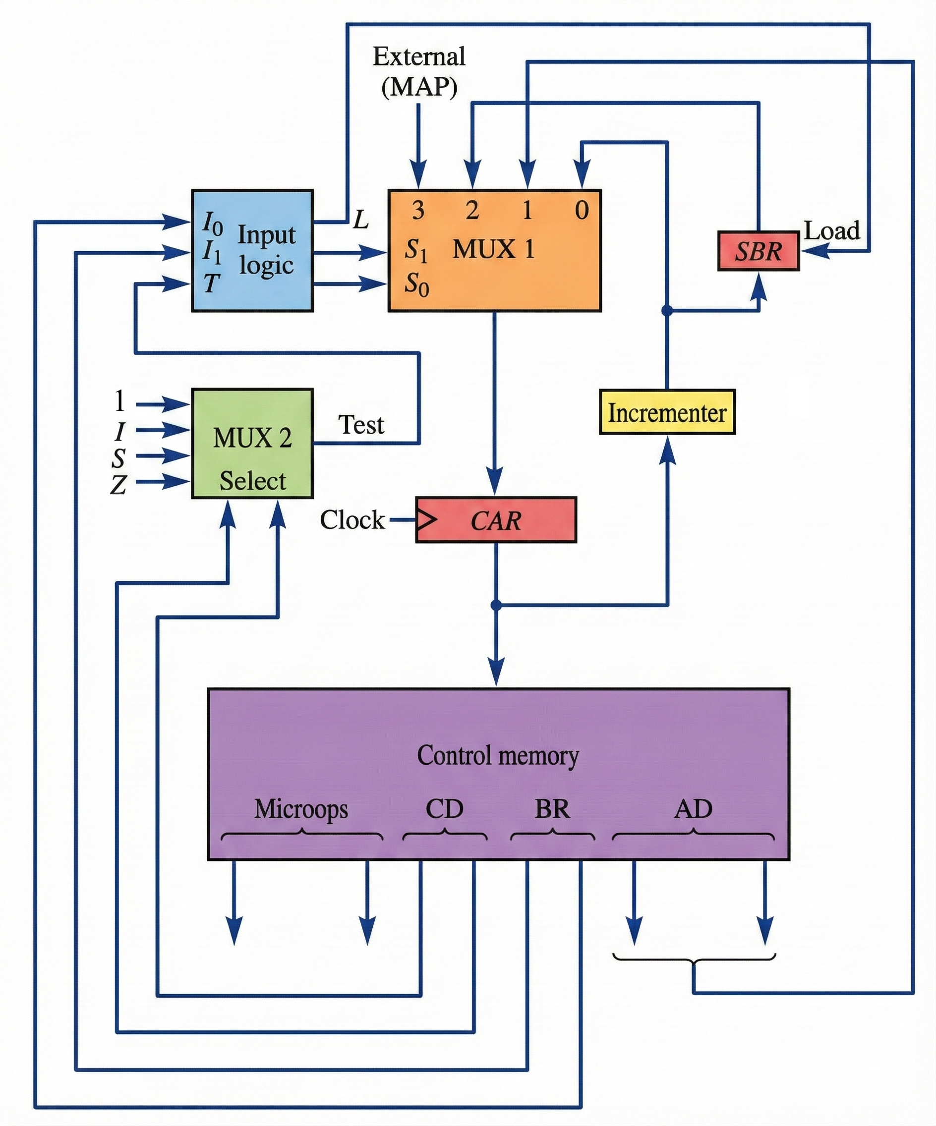
The microprogram sequencer presents an address to the control memory so that a microinstruction may be read and executed. The next-address information determines which microinstruction will be loaded into the control address register (CAR).
Address Source Selection
The sequencer can select addresses from multiple sources:
Sequencer Operations
- Increment: CAR = CAR + 1
- Branch: Jump to specified address
- Call: Save return address in SBR, jump to subroutine
- Return: Load address from SBR to CAR
- Load from external: Map instruction to starting address
Microprogram Counter Simulator
Current Address (CAR): 0000
Subroutine Register (SBR): ----
Control Path Selection
The sequencer uses a multiplexer (MUX 1) to select an address from one of four sources and routes it into CAR. A second multiplexer (MUX 2) tests the selected status bit, and the result is applied to an input logic circuit.
The output from CAR provides three possible address sources:
- Address field of present microinstruction
- Output of SBR (for return from subroutine)
- External source that maps instruction opcode
Circuit Diagram
Input Logic Circuit
Truth Table Analysis
The input logic circuit has three inputs (I₁, I₀, T) and three outputs (S₁, S₀, L). The circuit determines the path through which control information flows.
| BR Field | Input | MUX 1 | Load SBR | ||||
|---|---|---|---|---|---|---|---|
| BR₁ | BR₀ | I₁ | I₀ | T | S₁ | S₀ | L |
| 0 | 0 | 0 | 0 | 0 | 0 | 0 | 0 |
| 0 | 0 | 0 | 0 | 1 | 0 | 1 | 0 |
| 0 | 1 | 0 | 1 | 0 | 0 | 0 | 0 |
| 0 | 1 | 0 | 1 | 1 | 0 | 1 | 1 |
| 1 | 0 | 1 | 0 | × | 1 | 0 | 0 |
| 1 | 1 | 1 | 1 | × | 1 | 1 | 0 |
Boolean Functions
The simplified Boolean functions for the input logic circuit are:
S₁ = I1
S₀ = I1I0 + I1T
L = I1I0T
Operation Modes
I₁I₀ = 00 (Increment CAR)
The circuit increments CAR for normal sequential execution. When T=1, the BR address is loaded into CAR.
I₁I₀ = 01 (Call Subroutine)
Current CAR value is saved to SBR. When status bit T=1, BR address transfers to CAR.
I₁I₀ = 10 (Return from Subroutine)
The address from SBR is transferred to CAR, completing the return operation.
I₁I₀ = 11 (External Mapping)
An external address maps the instruction opcode to the starting microinstruction address.
Circuit Implementation
The circuit can be constructed using:
- Three AND gates
- One OR gate
- One inverter
Note: The incrementer circuit is not a counter constructed with flip-flops. Instead, it's a combinational circuit using half-adder circuits cascaded together for efficient operation.