Computer Design Overview
The design of a basic computer involves translating operational specifications into actual logic circuits. This process transforms register transfer statements into hardware implementations.
🎯 Key Design Objectives
Transform register transfer statements into functional hardware circuits that can execute computer instructions efficiently.
Memory-reference Instructions
Register-reference Instructions
IR(i) = Bᵢ (i = 0, 1, 2, ..., 11)
r: SC ← 0
Input-output Instructions
IR(i) = Bᵢ (i = 6, 7, 8, 9, 10, 11)
p: SC ← 0
Memory Specifications
Click to see details
Memory Unit
4096 words
16 bits per word
Total capacity: 64KB
Hardware Components
🗃️ Registers (9 total)
- AR - Address Register
- PC - Program Counter
- DR - Data Register
- AC - Accumulator
- IR - Instruction Register
- TR - Temporary Register
- INPR - Input Register
- OUTR - Output Register
- SC - Sequence Counter
🔄 Flip-Flops (7 total)
- I - Indirect address bit
- S - Start/Stop
- E - Extended accumulator
- R - Interrupt Request
- IEN - Interrupt Enable
- FGI - Input Flag
- FGO - Output Flag
🔍 Decoders
- 3 x 8 Operation decoder (opcodes)
- 4 x 16 Timing decoder (T0-T15)
🚌 Common Bus System
- 16-bit common bus
- Facilitates data transfer
- Controlled by S2, S1, S0 inputs
Flow Chart for Computer Operation
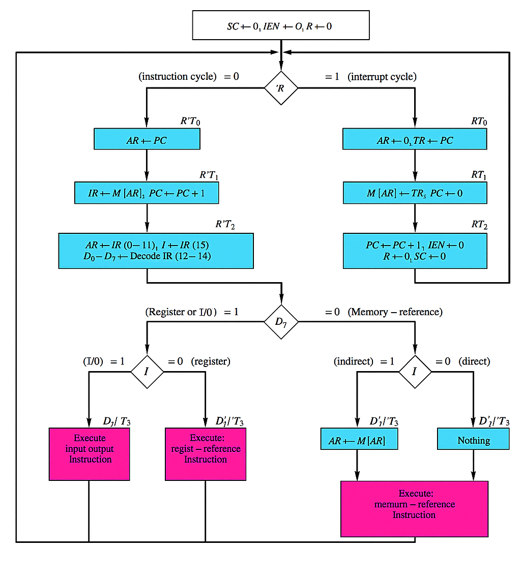
Control Unit Design
The control unit generates all necessary control signals for computer operation through decoders and logic gates.
🎛️ Control Functions
The control unit manages:
- Register control inputs (LD, INR, CLR)
- Memory read/write operations
- Flip-flop state changes
- Common bus register selection
- Arithmetic and logic operations
📊 Address Register (AR) Control Example
Clear Operation:
Load Operation:
Increment Operation:
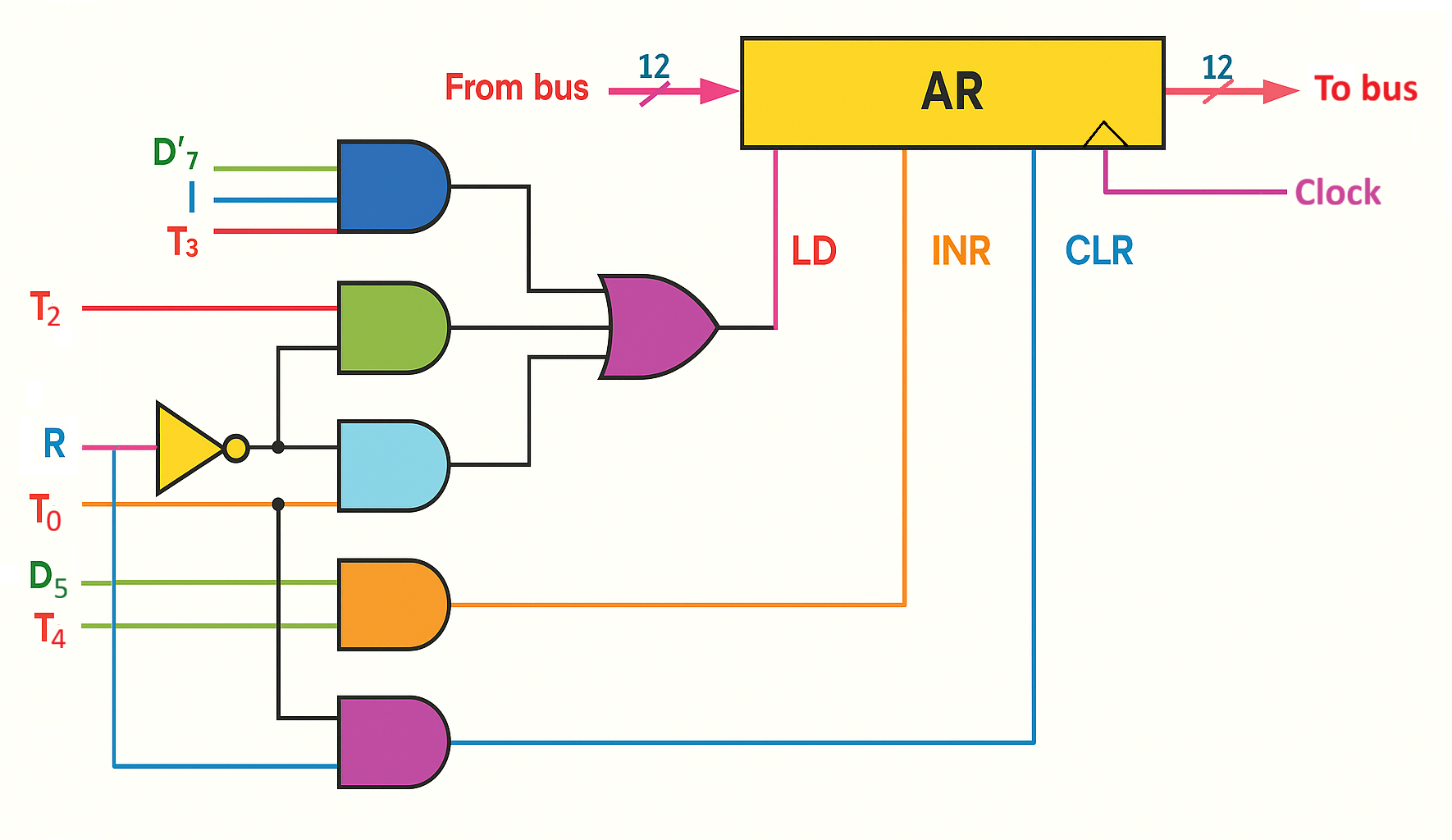
Control Signal Flow
Control signals are derived from register transfer statements and implemented as Boolean logic circuits.
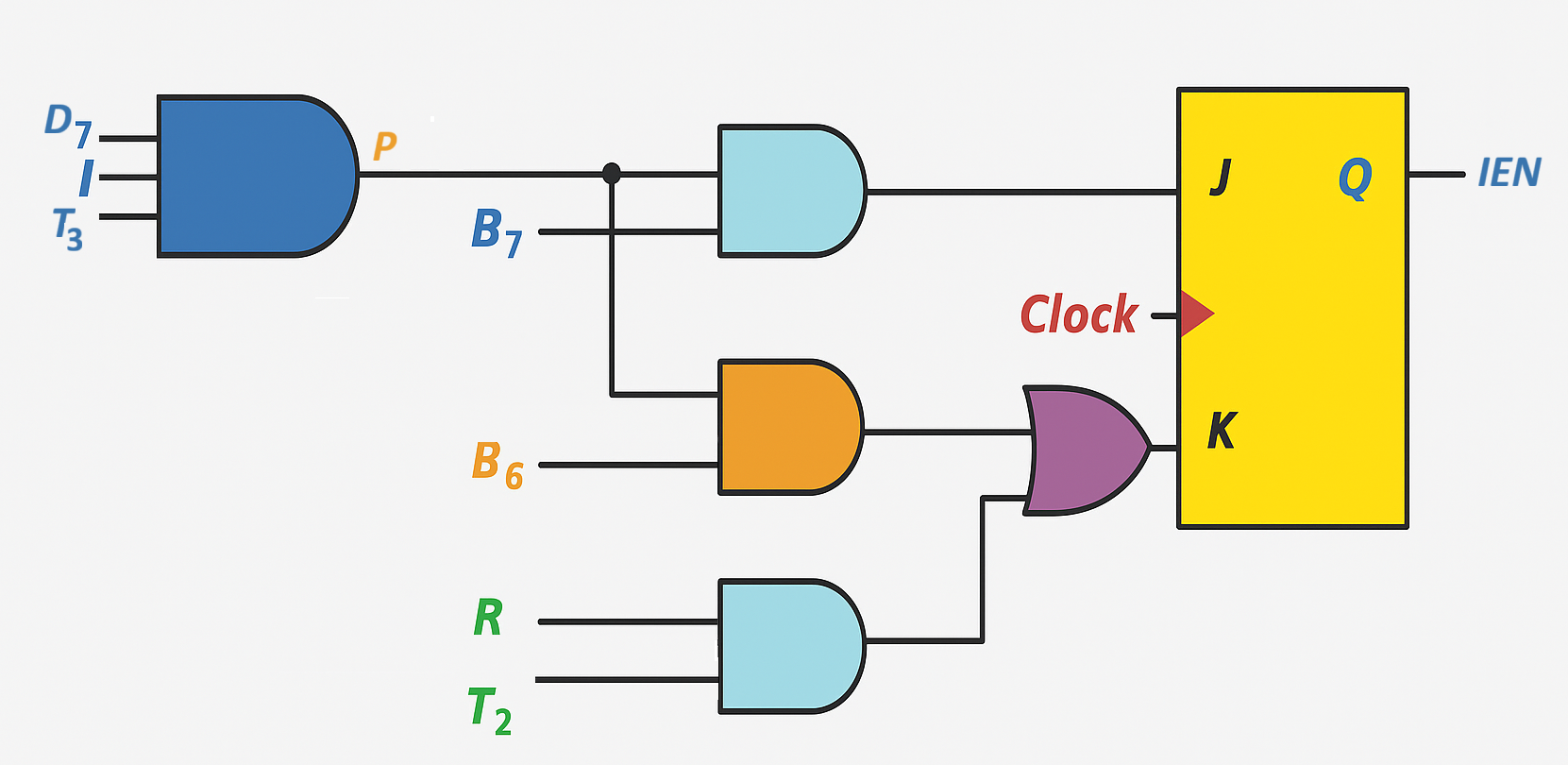
IEN Control
Interrupt Enable Logic
IEN Operations
pB7: IEN ← 1
pB6: IEN ← 0
RT2: IEN ← 0
🚌 Bus Control Logic
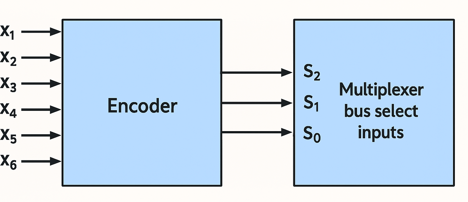
The 16-bit common bus is controlled by select inputs S2, S1, S0 of a multiplexer, determining which register's output is placed onto the bus. The control signals are derived from the register transfer statements.
Register Selection (S2, S1, S0)
- 001: Output of AR
- 010: Output of PC
- 011: Output of DR
- 100: Output of AC
- 101: Output of IR
- 110: Output of TR
- 111: Memory M[AR]
Bus Selection Inputs (S2, S1, S0)
- S0 = x1 + x3 + x5 + x7
- S1 = x2 + x3 + x6 + x7
- S2 = x4 + x5 + x6 + x7
Each binary value listed in the table corresponds to a Boolean variable xi, which activates the specific gate required to select the appropriate register or memory for the bus. When x1 = 1 to S₂S₁S₀ = 001 selects the AR register.
Encoder for Bus Selection Circuit
| Inputs | Outputs | Register Selected | ||||||||
|---|---|---|---|---|---|---|---|---|---|---|
| x1 | x2 | x3 | x4 | x5 | x6 | x7 | S2 | S1 | S0 | |
| 0 | 0 | 0 | 0 | 0 | 0 | 0 | 0 | 0 | 0 | None |
| 1 | 0 | 0 | 0 | 0 | 0 | 0 | 0 | 0 | 1 | AR |
| 0 | 1 | 0 | 0 | 0 | 0 | 0 | 0 | 1 | 0 | PC |
| 0 | 0 | 1 | 0 | 0 | 0 | 0 | 0 | 1 | 1 | DR |
| 0 | 0 | 0 | 1 | 0 | 0 | 0 | 1 | 0 | 0 | AC |
| 0 | 0 | 0 | 0 | 1 | 0 | 0 | 1 | 0 | 1 | IR |
| 0 | 0 | 0 | 0 | 0 | 1 | 0 | 1 | 1 | 0 | TR |
| 0 | 0 | 0 | 0 | 0 | 0 | 1 | 1 | 1 | 1 | Memory |
📊 Boolean Derivation Example
To determine the logic for each encoder input, it is necessary to find the control functions that place the corresponding register on the bus. For example, for x1:
D5T5: PC ← AR
x1 = D4T4 + D5T5
For x7, which represents memory selection:
Encoder for Bus Selection Inputs
Interactive Learning Demo
🚀 Computer Cycle Simulation
Click the button below to simulate a basic computer cycle:
💡 Key Learning Points
Hardware Translation
Register transfer statements become actual logic circuits
Control Logic
Boolean expressions control register operations
Systematic Design
Every microoperation has hardware implementation
🎓 Design Methodology Summary
The systematic approach ensures that every microoperation and control sequence defined for the basic computer has a corresponding hardware implementation, bridging the gap between theoretical computer architecture and practical digital circuit design.